
Discover the major manufacturing challenges and advanced process solutions for high frequency hybrid PCBs used in 5G communication, millimeter-wave radar, satellite systems, and RF applications. Learn about PTFE mixed lamination, plasma treatment, precision drilling, and impedance control.
/high-frequency-hybrid-pcb-manufacturing-solutions
High Frequency Hybrid PCB Manufacturing: Challenges, Processes, and Reliable Solutions
High frequency hybrid PCB technology has become a critical foundation for modern 5G communication systems, millimeter-wave radar, satellite communication equipment, aerospace electronics, and advanced RF testing devices. By combining low-loss RF materials such as Rogers RO4000 series and Taconic PTFE laminates with conventional FR-4 materials in a single multilayer stack-up, manufacturers can achieve both excellent signal integrity and cost-effective mechanical stability.
However, the manufacturing process of a high frequency hybrid PCB is far more complicated than standard multilayer PCB fabrication. Different material characteristics, thermal expansion mismatches, drilling instability, copper adhesion issues, and dimensional control all create major production challenges.
This article explores the key manufacturing difficulties of high frequency hybrid PCBs and the advanced engineering solutions used by leading PCB manufacturers today.
Why High Frequency Hybrid PCBs Matter
High frequency hybrid PCBs are widely used in applications that require stable RF performance and low transmission loss at frequencies above 1 GHz. Compared with fully PTFE-based circuit boards, hybrid constructions significantly reduce production cost while still maintaining excellent high-frequency electrical performance.
Typical applications include:
- 5G base stations
- Automotive radar systems
- Satellite communication modules
- Aerospace RF systems
- High-speed networking equipment
- Microwave antennas
- RF testing instruments
Because these systems operate at extremely high frequencies, even small manufacturing defects can severely impact insertion loss, impedance consistency, and signal reliability.
1. Lamination Challenges Caused by Material Differences
The biggest challenge in hybrid PCB manufacturing comes from the physical differences between PTFE-based RF materials and FR-4 substrates.
Thermal Expansion Mismatch
FR-4 typically has a Z-axis coefficient of thermal expansion (CTE) of around 50–70 ppm/°C, while PTFE materials may reach 200–300 ppm/°C. During lamination and soldering processes, this mismatch generates strong internal stress.
As a result, manufacturers may encounter:
- Delamination
- Board warpage
- Blistering
- Resin cracking
- Via reliability failure
Weak Bonding Interfaces
PTFE materials are chemically inert and naturally resistant to adhesion. Their soft surface structure creates weak bonding strength when combined with FR-4 layers.
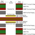
Hybrid PCB multilayer stack-up structure with PTFE and FR-4 layers
Advanced Lamination Solutions
Modern PCB factories solve these problems through highly controlled lamination processes.
Specialized Bonding Materials
Low-flow adhesive prepregs are commonly used between RF materials and FR-4 layers. These bonding films absorb stress while improving interface adhesion.
Multi-Stage Lamination Cycles
Instead of a simple press cycle, manufacturers use gradual temperature ramping and segmented pressure control to stabilize resin flow and reduce stress concentration.
Key process improvements include:
- Slow temperature increase
- Step-by-step pressure adjustment
- Controlled resin flow
- Extended curing time
Symmetrical Stack-Up Design
Engineers often place RF layers symmetrically within the PCB stack-up to minimize warpage during thermal cycling.
For more information about RF laminate behavior, manufacturers often reference technical resources from Rogers Corporation and Taconic Advanced Dielectric Division.
2. Precision Drilling and Hole Wall Quality Problems
Drilling hybrid PCBs is significantly more difficult than drilling standard FR-4 boards.
PTFE materials are soft and elastic, while glass-reinforced FR-4 is much harder. This combination causes drill bit instability during high-speed drilling.
Common defects include:
- Hole position deviation
- Rough hole walls
- Resin smear
- Burr formation
- Inconsistent hole diameter
PTFE also has an “elastic memory” effect, meaning the material can partially recover after drilling, causing dimensional instability.
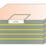 Precision drilling process for high frequency hybrid PCB vias
High-Precision Drilling Solutions
To maintain via reliability and hole accuracy, advanced PCB manufacturers apply several process optimizations.
Diamond-Coated Drill Bits
Diamond-coated or ultra-hard carbide drills improve cutting stability and reduce wear caused by fiberglass abrasion.
Optimized Drilling Parameters
Factories typically use:
- High spindle speed
- Low feed rate
- Multiple peck drilling cycles
- Controlled heat generation
Entry and Backup Materials
Aluminum entry sheets and composite backup boards help stabilize drilling quality while reducing exit burrs and deformation.
3. Copper Adhesion and Metallization Challenges
Copper plating reliability is considered the most critical process in high frequency hybrid PCB fabrication.
PTFE surfaces are naturally hydrophobic and chemically inert, making direct copper adhesion extremely difficult.
Without proper treatment, the PCB may suffer from:
- Hole wall copper cracking
- Barrel separation
- Blow holes
- Copper peeling
- Thermal stress failure
Plasma Surface Treatment Technology
Traditional desmear processes are not effective on PTFE materials. Therefore, advanced surface activation technologies are required.
Plasma Etching
Plasma treatment has become the industry-standard solution for PTFE activation.
Using CF4/O2 plasma gas mixtures, manufacturers create microscopic anchor structures on the PTFE surface while increasing surface energy.
Benefits include:
- Improved copper adhesion
- Better wettability
- Higher plating reliability
- Stronger chemical bonding
Pulse Plating Technology
Pulse electroplating ensures uniform copper thickness inside complex via structures and hybrid material interfaces.
This technology greatly improves:
- Current carrying capacity
- Thermal reliability
- Signal integrity
- Via consistency
Additional RF PCB process information can also be found through Microwaves & RF Magazine.

Plasma treatment process on PTFE PCB hole walls]
4. Dimensional Stability and Layer Registration
At millimeter-wave frequencies, transmission line geometry must be extremely precise.
Unfortunately, PTFE materials experience dimensional movement during:
- Lamination
- Drilling
- Chemical processing
- Thermal cycling
This creates serious layer alignment challenges.
Even tiny registration errors can affect:
- Controlled impedance
- Phase stability
- Return loss
- RF transmission efficiency
Solutions for Accurate Layer Alignment
Engineering Compensation
Manufacturers use historical shrinkage data to pre-compensate artwork dimensions before imaging.
Laser Direct Imaging (LDI)
LDI technology eliminates film distortion and improves registration accuracy to within ±15 μm.
High-Stability RF Materials
Ceramic-filled laminates such as Rogers RO4350B offer much better dimensional stability compared with pure PTFE materials.
Reliability Testing for High Frequency Hybrid PCBs
Reliable RF PCB production does not end after fabrication. Strict quality inspection and reliability validation are essential.
Non-Destructive Inspection
Modern factories use:
- X-ray inspection
- Ultrasonic scanning microscopy
- AOI inspection
- Cross-section analysis
Electrical Performance Testing
Vector network analyzers measure:
- Insertion loss
- Return loss
- Signal attenuation
- Impedance consistency
Thermal Reliability Testing
Common reliability tests include:
- 288°C solder float testing
- Thermal shock cycling
- Peel strength testing
- IST testing
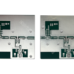
RF PCB reliability and thermal stress testing process
Conclusion
High frequency hybrid PCB manufacturing is one of the most demanding processes in the electronics industry. Successfully combining PTFE RF materials with conventional FR-4 requires deep expertise in material science, precision drilling, plasma surface treatment, multilayer lamination, and dimensional control.
As 5G infrastructure, autonomous driving systems, satellite communication, and millimeter-wave technologies continue to grow, the demand for reliable high frequency hybrid PCBs will increase rapidly. Manufacturers that can master these advanced fabrication techniques will play a crucial role in the future of wireless communication and high-speed electronic systems.