
High Frequency Multilayer PCB Lamination Alignment and Material Expansion Control for RF & 5G Applications
Learn how high frequency multilayer PCB manufacturers solve lamination alignment and material expansion issues in RF, 5G, millimeter-wave, and satellite communication PCBs. Discover advanced registration control, LDI imaging, mixed lamination technology, and dimensional compensation solutions.
 multilayer-pcb-lamination-registration-contro
High Frequency Multilayer PCB Lamination Alignment and Material Expansion Control
In the manufacturing of high frequency multilayer PCBs, lamination registration accuracy and material dimensional stability are among the most critical factors affecting product yield, signal integrity, and long-term reliability. As 5G communication systems, millimeter-wave radar modules, satellite communication devices, and advanced RF electronics continue evolving, multilayer high frequency PCB structures are becoming increasingly complex.
Higher layer counts, tighter impedance tolerances, and denser RF routing now demand significantly stricter registration control during PCB fabrication. Even small dimensional deviations can negatively impact microwave transmission performance, insertion loss, phase consistency, and antenna efficiency.
This article explores the root causes of material expansion and contraction in high frequency multilayer PCB production while analyzing modern solutions involving material matching, lamination optimization, dimensional compensation, and advanced imaging technologies.
Why Registration Control Is Critical in High Frequency PCB Manufacturing
Unlike conventional FR-4 multilayer boards, high frequency PCB structures often combine multiple materials with completely different thermal and mechanical properties.
Common RF laminate combinations include:
- Rogers RO4350B + FR-4
- PTFE laminates + FR-4
- Hydrocarbon ceramic materials + high-speed digital substrates
- Mixed RF and HDI stack-up structures
Because RF transmission lines operate at extremely high frequencies, any layer misalignment can directly affect:
- Controlled impedance
- Signal phase stability
- Insertion loss
- Return loss
- Via reliability
- Antenna consistency
For standard multilayer PCBs, interlayer registration tolerance is usually controlled within ±75 μm to ±125 μm. However, high frequency multilayer PCBs often require alignment accuracy within ±50 μm, while advanced HDI RF boards may demand precision below ±25 μm.
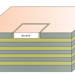
 High frequency multilayer PCB stack-up and registration alignment structure
Root Causes of Material Expansion and Shrinkage
1. Large Differences in Thermal Expansion Coefficient (CTE)
The biggest challenge in mixed high frequency PCB lamination comes from the significant CTE mismatch between RF materials and standard FR-4 substrates.
For example:
- FR-4 Z-axis CTE: approximately 50–70 ppm/°C
- PTFE material Z-axis CTE: approximately 200–300 ppm/°C
During lamination and reflow soldering, these materials expand and contract at completely different rates.
This leads to:
- Layer stress concentration
- Dimensional deformation
- Warpage
- Delamination
- Registration offset
For example, the thermal expansion difference between Rogers RO4350B and conventional FR-4 can exceed 50 ppm/°C. In mixed lamination structures, this can easily create global dimensional distortion or localized deformation.
2. Core Material Expansion Accumulation
PCB core materials experience dimensional movement during multiple thermal and chemical processes, including:
- Etching
- Lamination
- Baking
- Surface treatment
- Drilling
Changes in humidity and temperature further increase dimensional instability.
Since different laminate materials expand differently, the final position of each inner-layer circuit pattern may deviate from its original design coordinates after multilayer lamination.
This accumulated movement becomes increasingly difficult to control as layer counts increase.
Key Technologies for High Frequency PCB Registration Control
1. Inner Layer Artwork Compensation
Modern PCB manufacturers use scale factor compensation to offset predictable material expansion and shrinkage.
Before inner-layer imaging, the PCB artwork is intentionally enlarged or reduced according to historical dimensional movement data collected from specific materials and process conditions.
This allows the final laminated board to return to the correct design dimensions after thermal processing.
Compensation databases are typically established based on:
- Material type
- Board thickness
- Layer count
- Lamination cycle
- X/Y directional expansion behavior
This is especially important because many RF laminates exhibit strong anisotropic dimensional behavior.
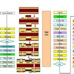
PCB artwork dimensional compensation process
2. High-Precision Lamination Positioning Systems
Mechanical positioning systems play a major role in multilayer registration accuracy.
Two-Pin Positioning
Commonly used for conventional multilayer PCB production.
Four-Pin or Slot Positioning Systems
For high layer count RF boards, manufacturers increasingly use:
- Four-slot positioning systems
- Pin-Lam technology
- Rivet-assisted alignment structures
These systems significantly improve dimensional stability during lamination and help maintain registration accuracy within ±25 μm.
This level of precision is especially important for:
- Millimeter-wave RF circuits
- HDI RF boards
- High-density antenna arrays
- Automotive radar modules
3. Mixed Lamination Interface Optimization
One of the biggest challenges in high frequency hybrid PCB manufacturing is maintaining reliable bonding between different substrate systems.
For example:
- Rogers RO4350B + FR-4
- PTFE + epoxy-based prepregs
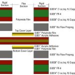
To improve interface reliability, manufacturers often insert transition layers between dissimilar materials.
Low-CTE Transition Materials
Ceramic-filled prepregs or specially formulated bonding films help smooth the CTE transition between RF laminates and FR-4.
This approach can reduce interlayer stress by more than 60%.
Optimized Lamination Profiles
Advanced lamination control includes:
- Gradual temperature ramping
- Segmented pressure adjustment
- Extended resin flow stages
- Controlled cooling cycles
These techniques reduce stress concentration and improve multilayer bonding strength.
For additional technical information about RF laminate systems, engineers often reference resources from Rogers Corporation and AGC Electronics Materials Division.
Advanced Solutions for High Frequency PCB Manufacturing
Modern high frequency PCB factories now implement comprehensive process control systems to improve registration stability and manufacturing yield.
Material Pre-Treatment
Before lamination, multilayer RF boards are typically vacuum baked at approximately 80°C for several hours to remove moisture completely.
PTFE materials may also undergo surface activation treatment to improve prepreg adhesion and interlayer bonding reliability.
Step-Controlled Lamination Process
Instead of using a single heating profile, advanced PCB manufacturers use multi-stage lamination cycles.
Benefits include:
- Uniform material heating
- Reduced localized stress
- Improved resin distribution
- Better layer bonding consistency
This process helps maintain interlayer bonding strength above 1.2 kN/m.
Laser Direct Imaging (LDI)
LDI technology has become increasingly important in high frequency multilayer PCB manufacturing.
Compared with traditional film exposure methods, LDI provides:
- Higher imaging precision
- Reduced film expansion error
- Better registration accuracy
- Improved fine-line capability
Using LDI, manufacturers can control line width tolerance within ±0.005 mm.
[Image Placeholder – Laser Direct Imaging process for high frequency PCB fabrication]
Full-Process Inspection and Verification
High frequency multilayer PCB manufacturing requires strict quality verification throughout the entire process.
X-Ray Inspection
X-ray systems verify via-to-pad alignment and internal registration accuracy.
Typical control targets include:
- Registration error below ±50 μm
- Accurate blind via positioning
- Layer alignment verification
Peel Strength Testing
Critical RF boards often undergo 100% peel strength testing to verify copper adhesion reliability.
Signal Integrity Validation
High-speed RF transmission channels are tested using vector network analyzers to evaluate:
- Insertion loss
- Return loss
- Impedance consistency
- Phase stability
Additional PCB process standards and testing references can also be found through IPC Association Connecting Electronics Industries.
Conclusion
As 5G infrastructure, millimeter-wave communication, satellite internet, and automotive radar systems continue advancing, the complexity of high frequency multilayer PCB manufacturing will only increase.
Among all manufacturing challenges, lamination registration control and material expansion management remain two of the most critical factors influencing RF performance and product reliability.
Through advanced dimensional compensation, precision positioning systems, optimized mixed-material lamination, LDI imaging, and full-process quality verification, modern PCB manufacturers can now achieve the ultra-tight tolerances required for next-generation RF and microwave applications.
For engineers developing high frequency multilayer PCBs, close collaboration with both laminate suppliers and PCB fabrication experts remains essential to achieving stable performance and long-term reliability.