
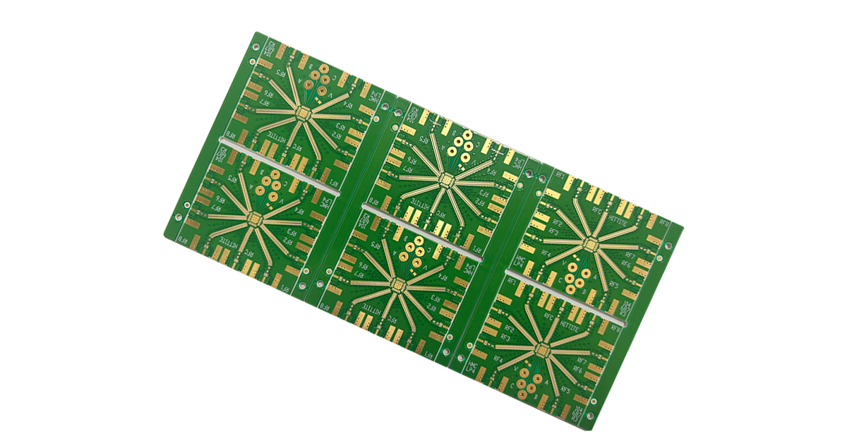
During high-frequency PCB design and manufacturing, due to the unique properties of high-frequency materials and special processing requirements, specific wiring suggestions should be followed to ensure the rationality of the board’s design and production.
When connecting analog ground, digital ground, and other ground lines to a common ground, high-frequency ferrite beads or direct isolation should be used, with single-point interconnection at appropriate locations. The ground potential of high-frequency digital signals is often inconsistent, leading to voltage differences. Additionally, high-frequency digital signal ground lines typically contain rich harmonic components. If digital and analog grounds are directly connected, these harmonics can couple into analog signals through the ground line, causing interference. Therefore, high-frequency digital ground and analog ground should be isolated, with interconnection achieved through single-point connections or high-frequency ferrite beads.
1. Ensure Proper Signal Impedance Matching
Impedance mismatches during signal transmission cause reflections, distorting the signal and leading to fluctuations near logic thresholds.
To minimize reflections:
- Match the load impedance with the transmission line’s characteristic impedance.
- Avoid abrupt bends or width changes in PCB traces to maintain impedance continuity.
Key High-Speed PCB Routing Rules:
- USB Routing: Requires differential pairs (trace width: 10 mil, spacing: 6 mil). Keep ground at least 6 mil from signal lines.
- HDMI Routing: Requires differential pairs (trace width: 10 mil, spacing: 6 mil). Maintain >20 mil spacing between differential pairs.
- LVDS Routing: Requires differential pairs (trace width: 7 mil, spacing: 6 mil) to control impedance at 100Ω ±15%.
- DDR Routing:
- DDR1: Avoid vias where possible. Maintain uniform trace width/spacing (follow the 2W rule to reduce crosstalk).
- DDR2+: Ensure equal trace lengths for high-speed data lines to maintain impedance matching.
2. Maintain Signal Integrity
Prevent ground bounce caused by improper ground plane splitting.
3. Minimize Crosstalk from Parallel Traces
Crosstalk—unintended coupling between adjacent traces—is critical in high-frequency PCBs. Factors like PCB layer stackup, trace spacing, driver/receiver characteristics, and termination affect crosstalk.
Reducing Crosstalk:
- Insert a ground plane or ground trace between high-risk parallel traces.
- Place a solid ground layer beneath parallel traces to absorb interference.
- Increase spacing between traces and minimize parallel run lengths.
- Route clock lines perpendicular to critical signals (not parallel).
- On adjacent layers, ensure traces run orthogonally (90°).
- For clock signals (prone to crosstalk due to fast edges):
- Surround with ground traces and ground vias to reduce parasitic capacitance.
- Use low-voltage differential signaling (LVDS) with ground shielding.
- Avoid floating unused input pins—terminate to ground or power (which acts as ground at high frequencies). Floating pins act as antennas, increasing EMI.