
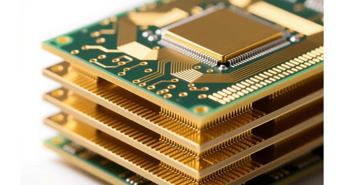
The longstanding industry perception that “the best high-frequency PCB materials must be imported” is undergoing a significant shift. Domestic suppliers have achieved large-scale substitution in mid-to-low frequency applications and made breakthroughs in specific advanced materials. However, the core technological battle for next-generation mmWave communications and top-tier AI computing substrates continues.
I. The Evolving Landscape: From Following to Competing
Performance gaps in key metrics for domestic high-frequency laminates were once a reality. After sustained R&D investment, domestic materials now firmly serve the mainstream market.
In the widely deployed Sub-6GHz spectrum for 5G infrastructure, core electrical parameters—dielectric constant (Dk) and dissipation factor (Df)—of products from leading Chinese suppliers are competitive with international equivalents. They adequately meet commercial requirements and have gained substantial domestic market share through cost and supply chain advantages, enhancing supply chain security for network equipment.
A more strategic breakthrough is occurring upstream. In ultra-low profile (HVLP) copper foil—a critical material for minimizing signal loss at high frequencies—a domestic producer has successfully developed HVLP5-grade foil with world-class surface roughness. This material is now supplied to leading global PCB manufacturers. Progress in localizing high-performance electronic resins, another once-monopolized upstream segment, is also accelerating.
II. The Unconquered Frontiers: mmWave and Extreme Performance
Despite this progress, imported materials maintain a stronghold in two demanding, high-value segments where performance margins are exceptionally thin.
First is the mmWave domain (≥30GHz). Applications like automotive radar, satellite links, and future 6G front-ends demand laminates with extraordinary consistency and ultra-low, stable loss. Minute variations in material properties can critically degrade system performance. The capability to mass-produce and reliably certify materials for these frequencies remains concentrated with a few international material science leaders.
Second is the frontier of AI server substrates and ultra-high-speed interconnects (≥112Gbps). Next-generation substrates for CPUs, GPUs, and switch chips require ultra-low-loss materials (often termed “M-series” grades). While domestic R&D can achieve similar lab specs, closing the gap in mass-production consistency, long-term reliability data, and acceptance by global flagship chip developers represents a longer-term challenge requiring deep customer collaboration and iteration.
III. The Deeper Hurdles: Advanced Processes and Ecosystem Gaps
Manufacturing capability extends beyond material availability. Transforming advanced laminates into functional boards involves complex process bottlenecks that are now central to the localization effort.
Sophisticated Process Mastery is Key. Manufacturing PCBs for AI servers, which may have over 30 layers and aspect ratios above 14:1, requires exceptional control over processes like pulse plating for uniform through-hole copper deposition. Similarly, hybrid builds combining high-speed, high-frequency, and standard materials within a single stack-up (“mixed lamination”) pose significant challenges in managing coefficient of thermal expansion (CTE) mismatch to prevent delamination.
Dependence on Specialized Tools. The production and validation of these advanced boards rely on high-end equipment, such as advanced laser direct imaging (LDI) systems for ultra-fine line patterning and high-frequency vector network analyzers (VNAs) for accurate signal integrity measurement. The highest-performance tiers of this equipment still originate from overseas, which can constrain rapid process development and precision.
IV. The Path Forward: Collaborative Definition and Ecosystem Integration
Achieving leadership requires moving beyond component substitution to integrated innovation and standard-setting.
The most effective path involves early and deep collaboration between PCB fabricators, OEMs, and upstream material scientists. Instead of selecting from standard catalog materials, leading players can co-define and co-develop application-specific materials, starting at the chemical formulation level—a model proven in global advanced electronics ecosystems.
Concurrently, industry players must transition from adhering to existing standards to actively shaping new ones, particularly for emerging domains like mmWave, terahertz, and next-generation signal integrity testing. Gaining influence in standards bodies is crucial for long-term competitiveness.
Conclusion
The localization journey for high-frequency PCBs has moved from possibility to widespread reality in mainstream applications. The current competition has evolved into a broader contest encompassing process excellence, control of the equipment chain, and influence over technical standards. As the industry marches toward 6G and advanced computing, success will belong to those who build cohesive, vertically synergistic innovation ecosystems capable of mastering the entire value chain from molecules to final systems.