
PCB stack-up is not simply an arrangement of layers. It is a systematic design of copper layers, dielectric layers, cores, prepregs, ground planes, and power planes. A well-designed stack-up can reduce EMI, control impedance, improve power integrity, and enhance the manufacturability of HDI, high-speed, high-frequency, and rigid-flex PCBs.
What Is PCB Stack-Up?
PCB stack-up refers to the sequence and thickness configuration of all internal board layers, including copper foil, core, prepreg, signal layers, power planes, and ground planes. It directly affects transmission line impedance, return paths, board thickness, tolerance, thermal performance, and cost.
For high-frequency PCBs, high-speed PCBs, HDI PCBs, and RF/microwave PCBs, the stack-up should be defined before layout, not added as a final manufacturing detail.
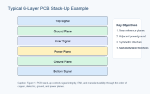
Caption: Figure 1. Typical PCB stack-up structure: signal layers should be placed close to continuous reference planes, while adjacent power and ground planes help reduce noise。
Alt: Typical six-layer PCB stack-up diagram showing the arrangement of signal layers, ground planes, power planes, and dielectric layers.
Why Does Stack-Up Design Affect Signal Integrity?
Impedance, Return Path, and EMI
The return current of high-speed signals flows along the nearest reference plane. If a signal layer does not have a continuous ground plane, or if the signal crosses a split power plane, reflection, crosstalk, ground bounce, and radiation can easily occur.
Impedance control depends not only on trace width, but also on copper thickness, dielectric thickness, Dk/Df, surface copper roughness, and the actual thickness after lamination. Therefore, designers should provide target impedance values and tolerances, while the manufacturer verifies them through material selection and TDR testing.
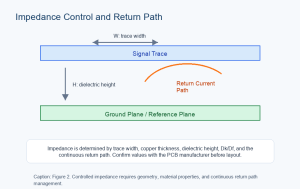
Caption: Figure 2. Impedance control and return path: geometry, dielectric properties, and reference plane continuity must be managed together.
Alt: Impedance control and return path diagram showing trace width, dielectric thickness, reference ground plane, and return current.
Key Rules for High-Speed and High-Frequency PCB Stack-Up
- Place high-speed or RF signal layers next to solid ground planes to reduce loop area and EMI.
- Avoid stacking adjacent signal layers directly together; use orthogonal routing or add ground plane isolation when necessary.
- Keep power and ground planes close together to create a low-impedance PDN, combined with proper decoupling capacitors.
- Maintain stack-up symmetry and balanced copper distribution to reduce warpage and board deformation.
- For HDI designs, control lamination cycles and select blind vias, buried vias, stacked vias, or staggered vias properly.
- For rigid-flex PCBs, place flexible layers in the middle and keep vias and components away from bending areas.
- For high-frequency hybrid stack-ups, pay attention to material CTE, Dk/Df, and lamination compatibility.
What Must Be Clearly Defined in DFM Files?
Manufacturing drawings should clearly specify layer sequence, material model, core/prepreg thickness, copper thickness, total board thickness and tolerance, impedance trace locations, dielectric constant, dissipation factor, surface finish, solder mask color, via structure, IPC class, and testing requirements.
Missing impedance data, high-aspect-ratio vias, unbalanced copper distribution, or asymmetric stack-up can increase the risk of rework, warpage, and performance failure.
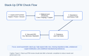
Caption: Figure 3. Stack-Up DFM inspection process: confirming layer count, materials, impedance, vias, and manufacturing tolerances step by step.
Alt: PCB stack-up DFM inspection flowchart including layer count, materials, impedance, vias, and manufacturing tolerances.
Conclusion
An excellent PCB stack-up design is essentially a balance between electrical performance, mechanical reliability, and manufacturing capability. For high-speed, high-frequency, HDI, rigid-flex, and hybrid PCBs, confirming the stack-up, impedance, and materials as early as possible helps reduce EMI, crosstalk, lamination risk, and mass production cost.