
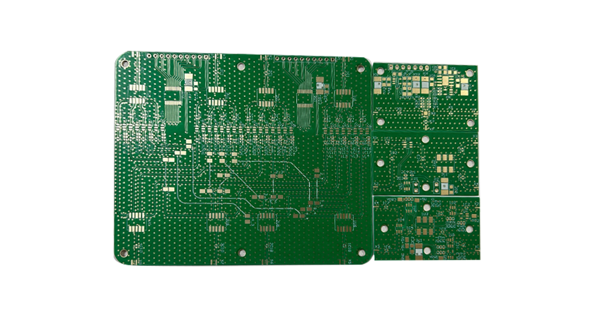
In PCB design for millimeter-wave (mmWave) frequency bands (typically 30GHz to 300GHz), copper surface treatment critically impacts signal integrity, insertion loss, and impedance control. With the rapid development of 5G communications, automotive radar, and high-speed digital applications, engineers face the challenge of choosing between low-roughness copper and reverse-treated foil. This article provides an in-depth analysis of these two copper treatment technologies, comparing their characteristics, advantages, limitations, and application scenarios to guide high-frequency PCB material selection.
1. Special Requirements for Copper Foil in mmWave Applications
Millimeter-wave signals exhibit short wavelengths, weak penetration, and high sensitivity to conductor loss, imposing three core requirements on PCB copper foil:
- Surface Roughness Control: Copper surface irregularities increase skin effect loss. At 76GHz, every 1μm increase in roughness may introduce an additional 0.1dB/cm loss.
- Interfacial Bonding Strength: High-frequency laminates (e.g., RO4835, Tachyon-100G) require strong adhesion between copper and dielectric layers to prevent microcracks during multilayer lamination.
- Etching Precision: Fine-line circuits (≤50μm trace/space) demand post-etch copper edge burrs below 5μm.
2. Low-Roughness Copper Foil Technology
2.1 Process Characteristics
Optimized electrolytic copper deposition employs ultra-smooth cathode drums and specialized additives to refine copper crystal grain size below 2μm, achieving surface roughness (Ra) of 0.3-0.5μm—over 60% lower than standard electrodeposited copper (Ra 1.2-2μm).
2.2 mmWave Performance Advantages
- Loss Reduction: Demonstrates 15%-20% lower insertion loss at 60GHz compared to standard foil
- Impedance Stability: Limits impedance variation to ±2Ω (@100Ω differential) from roughness-induced fluctuations
- Process Compatibility: Suitable for laser drilling (<100μm vias) and modified semi-additive process (mSAP)
2.3 Limitations
- Cost Premium: 30%-50% more expensive than conventional copper
- Adhesion Challenges: Requires specialized surface treatments (e.g., brown oxide or nano-silane coupling agents)
3. Reverse-Treated Copper Foil Technology
3.1 Structural Innovation
Reverse-treated foil inverts the traditional copper foil configuration—the original smooth side becomes the bonding surface to the substrate, while the matte side serves as the circuit formation surface after specialized treatment.
3.2 High-Frequency Performance
- Dual-Surface Optimization: Circuit-side Ra ≤0.8μm; bonding-side Ra 1.5-2μm ensures adhesion
- Balanced Loss Profile: At 28GHz, performance sits between standard and low-roughness copper
- Cost Efficiency: 20%-30% cheaper than low-roughness alternatives
3.3 Technical Constraints
- Narrow Process Window: Requires lamination temperature control within ±5°C
- Etching Compensation: Asymmetric roughness may necessitate 10% additional etch compensation
4. Selection Decision Tree
4.1 Prioritize Low-Roughness Copper When:
- Designing phased-array antenna feed networks ≥60GHz
- Requiring insertion loss <0.5dB/cm for mmWave transmission lines
- Using ultra-thin dielectrics (≤100μm) in multilayer boards
4.2 Opt for Reverse-Treated Foil When:
- Developing 24-40GHz automotive radar PCBs
- Producing cost-sensitive high-volume products (>1,000㎡ annual usage)
- Implementing hybrid designs needing FR4 process compatibility
5. Emerging Trends
- Hybrid Architectures: Combining low-roughness copper for critical signal layers with reverse-treated foil in power planes
- Atomic-Level Polishing: Chemical-mechanical polishing (CMP) achieving sub-0.1μm Ra
- Smart Roughness Distribution: Region-specific roughness tuning (e.g., lower Ra in bend sections)
Conclusion
Selecting copper foil for mmWave PCBs requires balancing frequency range, loss budget, cost constraints, and manufacturing capabilities. Low-roughness copper delivers superior performance at ultra-high frequencies, while reverse-treated foil offers a cost-effective compromise. Early-stage 3D EM simulations (HFSS/CST) comparing field distributions across foil types—combined with prototype testing—are recommended for final decisions. As 6G research advances, copper surface treatments will continue evolving toward nanometer-scale precision.