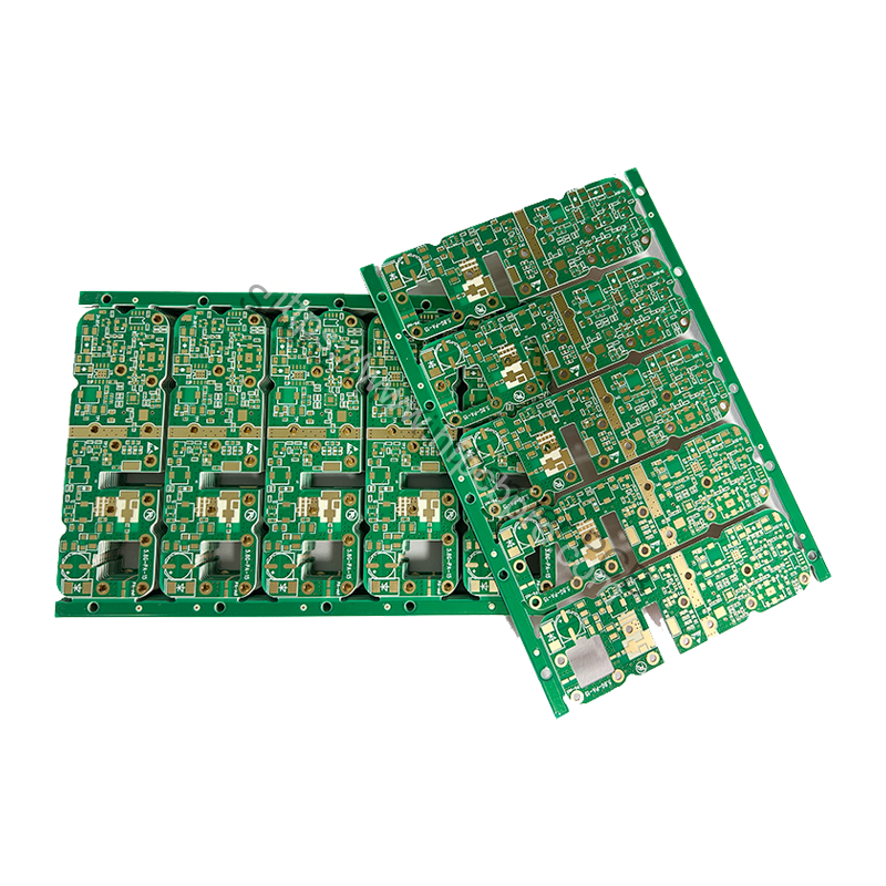
Key Considerations for High-Frequency PCB Design and Fabrication
I. Design Phase: Focusing on Signal Integrity and Electromagnetic Compatibility
- Material Selection
- Low dielectric constant (Dk) and low loss tangent (Df): Prioritize materials with Dk < 3.5 and Df < 0.002 (e.g., Rogers RO4003C, polytetrafluoroethylene (PTFE)) to minimize signal delay and attenuation.
- Copper foil type: Use ultra-low profile copper foil (HVLP/RTF) to reduce skin effect losses and enhance high-frequency performance.
- High-temperature resistance: Select materials with Tg > 170°C and CTE < 50 ppm/°C (e.g., Nelco N4000-13) for high-temperature operating environments.
- Impedance Control
- Precise calculation: Use tools like Polar SI9000 to calculate target impedance (e.g., single-ended 50 Ω, differential 100 Ω) based on material Dk, trace width, and dielectric thickness.
- Transmission line types:
- Microstrip: Signal trace on the top layer with a solid ground plane below; simple design but susceptible to surface environment effects.
- Stripline: Signal trace sandwiched between two ground planes; offers better shielding and stable impedance but higher cost.
- Avoid impedance discontinuities: Use rounded or 45° angled corners, maintain equal length and spacing for differential pairs, and ensure symmetry in serpentine routing.
- Stack-up Design
- Adjacent signal and ground layers: Place high-frequency signal layers adjacent to ground layers to form stable return paths and reduce interference.
- Uniform layer thickness: Avoid uneven layer thickness to prevent impedance mismatch.
- Ground plane shielding: Add ground planes around sensitive areas to isolate external electromagnetic interference.
- Power and Ground Design
- Low-impedance power planes: Use a multilayer board structure with adjacent power and ground layers to form low-impedance loops.
- Decoupling capacitor placement: Position 0.1 μF ceramic capacitors + 10 μF tantalum capacitors near IC power pins to suppress power supply noise.
- Split ground handling: Connect digital and analog grounds at a single point using ferrite beads or 0 Ω resistors to avoid common-mode noise.
- Via Optimization
- Minimize via count: Each via introduces parasitic capacitance and inductance, potentially causing signal reflections.
- Backdrilling: Remove unused layer stubs to reduce resonant interference (especially critical for signals > 5 GHz).
- Via-in-pad design: Drill vias in pads and plate them to shorten signal paths.
- Layout Rules
- Short and straight traces: Keep high-frequency signal traces as short and straight as possible to reduce losses and delays.
- Keep away from noise sources: Route high-frequency traces away from clocks, power supplies, digital noise sources, and board edges.
- Compact layout of critical components: Place RFICs, antennas, filters, etc., close together to shorten interconnect lengths.
II. Fabrication Phase: Precision Processes and Material Adaptation
- Inner Layer Fabrication
- Pattern transfer accuracy: Use laser direct imaging (LDI) technology to achieve ±2 μm line width accuracy, avoiding deviations caused by thermal expansion/contraction in traditional photolithography.
- Etching control: Maintain side etching < 1 mil to prevent trace gaps and pinholes that affect performance.
- Lamination Process
- Vacuum lamination: Apply pressure of 300 ± 50 PSI and a temperature gradient ≤ 2°C/min to avoid interlayer bubbles and delamination.
- Layer alignment: Use an X-ray positioning system to achieve layer misalignment accuracy of ±25 μm, ensuring alignment between signal and ground layers.
- Drilling and Via Metallization
- Laser drilling: Use UV lasers (355 nm) to drill microvias (diameter 0.1 mm ± 3 μm) with a surface roughness Ra < 0.5 μm.
- Chemical copper deposition: Employ vertical continuous plating (VCP) technology to achieve uniform copper layer thickness of 80 μm in vias, reducing void defects.
- Solder Mask and Surface Finish
- Solder mask adhesion: Perform special pre-treatment for high-frequency boards (e.g., acid cleaning + baking at 90°C/30 min) to prevent blistering.
- Surface finish selection:
- Electroless nickel immersion gold (ENIG): Nickel layer 3-5 μm, gold layer 0.05-0.1 μm; offers good planarity and is suitable for high-frequency signal transmission.
- Immersion silver: Lower loss but prone to oxidation; requires strict packaging.
- Avoid HASL: Uneven surface increases high-frequency losses.
III. Testing Phase: Rigorous Verification of Signal Integrity
- Impedance Testing: Use a time-domain reflectometer (TDR) to measure transmission line impedance and ensure a tolerance of ±10%.
- S-Parameter Testing: Use a vector network analyzer (VNA) to test S11 (reflection coefficient) < -15 dB and S21 (transmission coefficient) > -3 dB to verify signal integrity.
- Thermal Stress Testing: Perform 3 IR reflow cycles (260°C ± 5°C) and check for a delamination rate < 5%.
- Simulation-Driven Design: Conduct signal integrity (SI), power integrity (PI), and electromagnetic compatibility (EMC) simulations during the design phase to optimize layout and parameters.
IV. Golden Rules for High-Frequency PCB Design and Fabrication
- Choose the right board: Low-loss, stable Dk materials are fundamental (e.g., Rogers RO4000 series).
- Calculate traces accurately: Precise control of transmission line impedance is crucial (use Polar SI9000 or ADS simulations).
- Manage vias effectively: Optimizing via design (backdrilling, via-in-pad) is a key challenge.
- Optimize layout: Keep traces short, straight, and away from noise sources; maintain a complete ground plane.
- Combine simulation and testing: Use simulations to predict issues and testing to verify performance; both are indispensable.