

Learn the complete high-frequency PCB customization process, from material selection and impedance control to manufacturing, testing, and quality assurance. Discover best practices for RF, microwave, 5G, and radar PCB projects.
High-Frequency PCB Customization Guide: From Material Selection to Mass Production
High-frequency PCB customization has become increasingly important as industries continue to adopt advanced technologies such as 5G communications, automotive radar, satellite navigation, aerospace electronics, and RF wireless systems. Unlike conventional PCB manufacturing, high-frequency PCB fabrication requires stricter control over material properties, signal integrity, impedance consistency, and production processes.
Even a small deviation in dielectric thickness, copper roughness, or drilling quality can significantly impact RF performance. Therefore, understanding the complete customization process is essential for achieving reliable and repeatable results.
This guide outlines every critical stage of high-frequency PCB customization and provides practical recommendations to help engineers avoid common manufacturing pitfalls.
I. Defining High-Frequency PCB Requirements
Every successful high-frequency PCB project begins with a clear definition of electrical and mechanical requirements.
Key Electrical Parameters
Before selecting materials or designing the PCB stackup, the following specifications should be confirmed:
- Operating frequency range
- Characteristic impedance requirements (50Ω, 75Ω, or custom values)
- Dielectric constant (Dk) and tolerance
- Dissipation factor (Df)
- Insertion loss budget
- Signal integrity requirements
- Thermal performance requirements
For RF and microwave applications, dielectric stability across different frequencies and temperatures is particularly important.

Image 1: High-frequency PCB used in 5G communication equipment and RF systems.
II. Selecting the Right High-Frequency PCB Material
Material selection is one of the most critical decisions in any high-frequency PCB project.
Common High-Frequency PCB Materials
| Material Type | Representative Products | Main Advantages |
|---|---|---|
| PTFE-Based | Rogers RO3000 Series, Taconic | Ultra-low loss, excellent RF performance |
| Hydrocarbon Ceramic | Rogers RO4000 Series | Good balance of performance and cost |
| Modified Epoxy | Panasonic, Isola | Cost-effective for medium-frequency applications |
| Ceramic-Filled PTFE | Rogers RO3000 Series | Superior thermal and dimensional stability |
Material Selection Considerations
When selecting a high-frequency PCB substrate, engineers should evaluate:
- Dielectric constant stability
- Loss tangent performance
- Thermal conductivity
- Copper foil adhesion
- Availability and lead time
- Glass transition temperature (Tg)
For detailed material data, engineers can consult:
III. High-Frequency PCB Design Considerations
Impedance Control Design
Controlled impedance is fundamental to RF PCB performance.
Best practices include:
- Using impedance simulation tools such as Polar SI9000
- Accounting for etching compensation
- Maintaining continuous reference planes
- Controlling dielectric thickness variation
Most RF designs require impedance tolerances within ±5%, while critical applications may require ±3% or tighter.
Signal Integrity Optimization
Signal integrity becomes increasingly important as frequencies rise.
Recommended design practices include:
- Minimizing via count
- Avoiding 90° routing corners
- Using smooth curves or 135° bends
- Maintaining tight differential pair matching
- Adding sufficient ground stitching vias
These techniques help reduce reflections, crosstalk, and radiation losses.
Image 2: Controlled impedance routing and differential pair design in a high-frequency PCB layout.
IV. Stackup Design for High-Frequency PCBs
A properly engineered stackup is essential for maintaining consistent impedance and minimizing signal loss.
Key Stackup Principles
- Symmetrical layer construction
- Controlled dielectric thickness
- Proper reference plane placement
- Low-loss prepreg selection
- Consistent copper distribution
Materials such as RO4450F and FR27 are commonly used prepregs in hybrid high-frequency PCB constructions.
Copper Foil Selection
For RF applications, rolled annealed copper generally provides better performance than standard electrodeposited copper due to its smoother surface profile.
Lower copper roughness directly contributes to reduced conductor loss at high frequencies.
V. Engineering Review Before Production
The engineering review stage serves as a critical bridge between design and manufacturing.
Manufacturability Review
Key checks include:
- Minimum trace width and spacing
- Annular ring requirements
- Via aspect ratios
- Layer registration capability
- Panel utilization efficiency
Potential manufacturing risks should be identified and corrected before production begins.
Surface Finish Selection
The choice of surface finish directly affects both RF performance and assembly reliability.
Common options include:
- Immersion Silver
- ENIG (Electroless Nickel Immersion Gold)
- OSP
- Hard Gold
For many RF applications, immersion silver is preferred due to its low insertion loss characteristics.
VI. Critical Manufacturing Process Controls
Drilling Process
PTFE-based materials are softer than conventional FR-4 laminates and require special drilling procedures.
Recommended practices include:
- Using new carbide drill bits
- Optimizing spindle speed and feed rate
- Increasing chip evacuation frequency
- Performing plasma cleaning after drilling
Through-Hole Metallization
PTFE materials have low surface energy, making copper deposition more challenging.
To ensure reliable plating:
- Plasma activation is recommended
- Sodium treatment may be required
- Copper thickness must be tightly controlled
Pattern Transfer and Imaging
Laser Direct Imaging (LDI) technology helps improve dimensional accuracy and minimizes artwork distortion caused by material expansion.
Etching Process
For high-frequency PCB manufacturing:
- Trace width tolerance should remain within ±10%
- Critical impedance traces may require ±0.5 mil control
- Sidewall profile should be carefully monitored
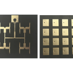
Image 3: Precision drilling, imaging, and etching processes during high-frequency PCB fabrication.
VII. Quality Inspection and RF Performance Verification
Traditional electrical testing alone is insufficient for high-frequency PCB validation.
Recommended Testing Methods
Impedance Testing
Time Domain Reflectometer (TDR) testing verifies controlled impedance performance across critical transmission lines.
Cross-Section Analysis
Cross-section inspection evaluates:
- Copper plating thickness
- Layer alignment accuracy
- Dielectric thickness consistency
- Via wall integrity
Thermal Reliability Testing
Tests include:
- Thermal cycling
- Solder float testing
- Reflow simulation
- Moisture resistance evaluation
RF Performance Verification
Advanced projects may require:
- Vector Network Analyzer (VNA) testing
- Insertion loss measurement
- Return loss testing
- Passive intermodulation (PIM) testing
VIII. Delivery, Packaging, and Storage
Proper handling after fabrication is equally important.
Recommended Packaging
High-frequency PCBs should be protected using:
- Vacuum-sealed packaging
- Anti-static bags
- Moisture barrier materials
- Rigid separators
Storage Recommendations
OSP-finished boards should typically be assembled within 72 hours after opening.
Gold-finished boards offer longer storage life but should still be protected from humidity and contamination.
Documentation Requirements
Professional PCB suppliers should provide:
- Impedance test reports
- Electrical test reports
- Cross-section analysis reports
- Material certificates
- Incoming inspection records
IX. Common High-Frequency PCB Issues and Solutions
| Common Issue | Root Cause | Recommended Solution |
| Impedance Variations | Over-etching, dielectric inconsistency | Improve etching and lamination control |
| Poor Via Metallization | Insufficient PTFE activation | Apply plasma treatment |
| Board Warpage | Asymmetrical stackup | Use balanced stackup design |
| Excessive Signal Loss | Rough copper foil, solder mask influence | Use rolled copper and selective mask openings |
| Soldering Blisters | Moisture absorption | Bake boards before assembly |
Conclusion
High-frequency PCB customization is a multidisciplinary process involving material science, RF engineering, manufacturing expertise, and rigorous quality control. From selecting the proper laminate to validating RF performance after fabrication, every stage influences the final electrical performance of the product.
Partnering with an experienced high-frequency PCB manufacturer can significantly reduce development risks, improve first-pass success rates, and shorten product development cycles. Early collaboration during the design phase often delivers the greatest long-term benefits for RF, microwave, and 5G communication projects.