
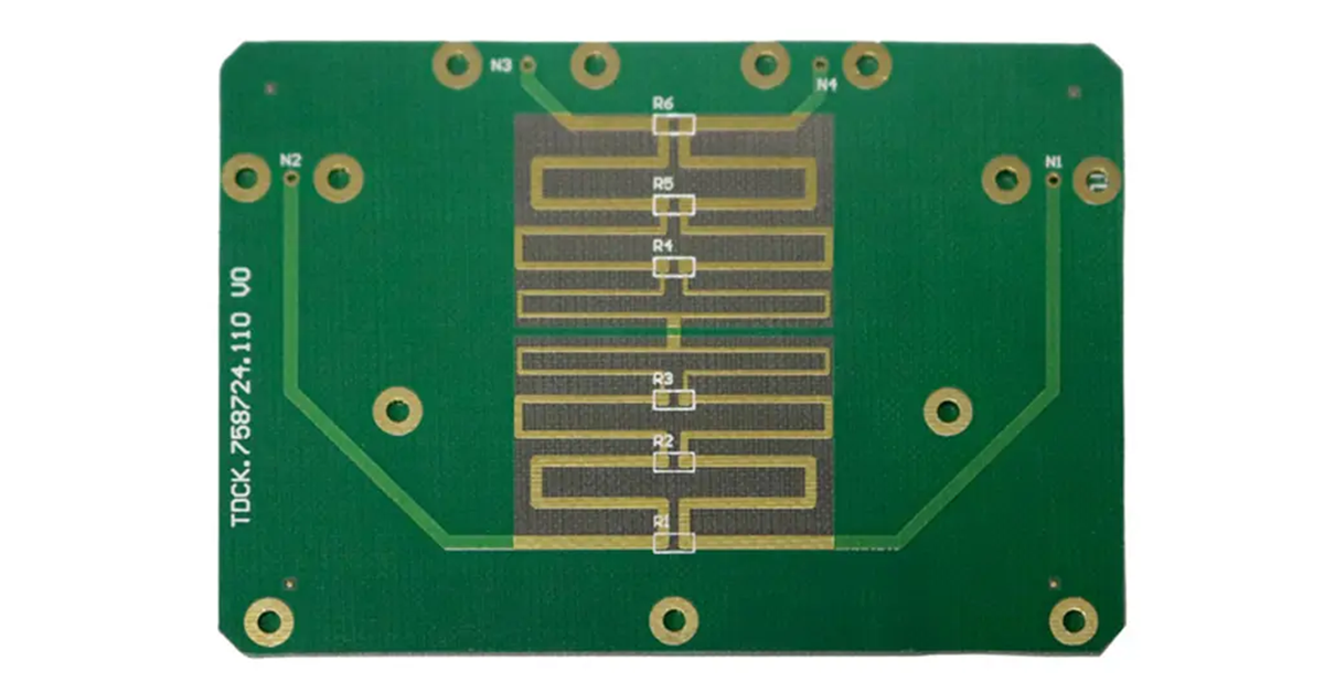
The Precision Challenge in Microstrip Design
In today’s rapidly evolving communication technologies, high-frequency PCB design has become a critical enabler for 5G, satellite communications, and radar systems. As a key focus for high-frequency RF PCB manufacturers, achieving impedance consistency in 0.05mm trace-width microstrip lines demands unprecedented precision. While such ultra-fine traces enable low-loss high-frequency signal transmission, they also introduce significant challenges in impedance control.
Gold-plated high-frequency PCBs are increasingly used in millimeter-wave applications, where microstrip impedance consistency directly impacts system stability. A 0.05mm trace width (comparable to a human hair’s diameter) means even minor PCB fabrication variations can cause substantial impedance shifts, degrading signal integrity.
Key Factors Affecting Impedance Consistency
1. Dielectric Material Selection
For 0.05mm microstrips, the dielectric constant (Dk) and its uniformity are critical. High-frequency applications require low-loss, thermally stable materials like Rogers or Taconic advanced composites, with Dk values typically between 2.2–3.5 and excellent board-wide consistency.
2. Copper Surface Treatment
Gold-plated high-frequency PCBs often use reverse-treated foil (RTF) or very-low-profile (VLP) copper, which provide smoother surfaces to minimize skin-effect losses. For 0.05mm traces, copper roughness must be below 1µm to ensure accurate impedance calculations.
3. Manufacturing Precision
Trace width tolerance, dielectric thickness control, and etch factors significantly impact impedance. A ±0.005mm deviation in a 0.05mm trace can cause 2–3Ω impedance shifts—unacceptable for high-speed designs.
Engineering Best Practices for Impedance Control
1. Precision Simulation in Design
Advanced EM simulation tools (HFSS, CST) must account for real-world variables:
- Copper thickness variations
- Dielectric layer tolerances
- Solder mask effects
2. Optimized Process Control
- Laser Direct Imaging (LDI) for 0.05mm trace accuracy
- Tightly controlled etching parameters (chemistry, temperature, spray pressure) to minimize undercut
- 100% automated optical inspection (AOI) for critical impedance lines
3. Material Pre- & Post-Treatment
- Pre-bake substrates to remove moisture
- Monitor production environment (temperature/humidity)
- Validate impedance with TDR (Time Domain Reflectometry) scanning
Testing & Validation Methods
1. High-Frequency Impedance Measurement
- Micro-probes or non-contact techniques for 0.05mm traces
- Vector Network Analyzers (VNA) with precision calibration for mmWave bands
2. Signal Integrity Analysis
- Eye diagram and bit-error-rate (BER) testing for real-world performance
- Collaboration between PCB manufacturers and end-users to correlate impedance with system performance
Future Trends in High-Frequency PCB Design
- Finer Traces (0.03mm and below) for 5G mmWave/THz applications
- Advanced Processes: Modified semi-additive (mSAP/amSAP) for ultra-fine lines
- AI-Driven Optimization: Machine learning to predict/manufacturing variations
- New Materials: Liquid crystal polymer (LCP) and low-loss modified epoxies
Conclusion
Achieving impedance consistency in 0.05mm microstrips requires high-frequency PCB manufacturers to master design, materials, process control, and testing. As 5G, aerospace, and defense push performance limits, gold-plated high-frequency PCBs will continue evolving to meet tomorrow’s ultra-high-speed demands.