
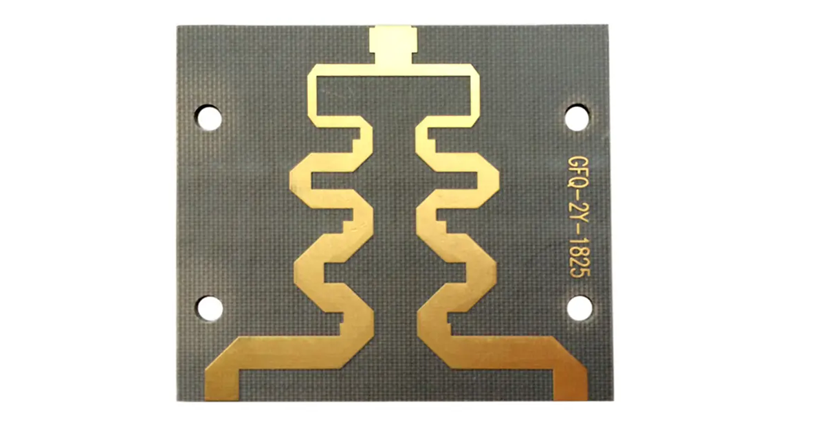
The Critical Process for 5G & Aerospace PCBs
F4B high-frequency laminates (Dk=2.65, Df=0.001) are increasingly combined with FR4 in multilayer designs to balance performance and cost. However, the CTE mismatch (16ppm/°C vs. 13-18ppm/°C) and resin incompatibility create unique challenges. This guide reveals proven techniques from leading RF PCB manufacturers to achieve reliable hybrid constructions.
3 Key Challenges in F4B/FR4 Hybrid Lamination
1. CTE Mismatch Risks
- Post-lamination warpage (>0.5% can cause assembly issues)
- Via reliability concerns under thermal cycling
2. Resin Flow Differential
| Material | Flow Temp | Gel Time |
|---|---|---|
| FR4 Epoxy | 110-140°C | 40-60min |
| F4B PTFE | 327°C+ | N/A |
3. Adhesion Requirements
- Peel strength must exceed 0.8N/mm
- Void content <0.1% at interfaces
Temperature Profile Optimization
Stage 1: Preheating (80-120°C)
- Goal: Gradual heat-up prevents FR4 pre-cure
- Best Practice:
- Ramp rate: 10°C/min (validated by Xinchenger)
- Hold at 100°C for 15min to equalize
Stage 2: Melt Phase (180-220°C)
- Critical Parameters:
- 185-190°C: FR4 full flow temperature
- 45min dwell time for complete filling
- Solution:
- Use TU-768 low-flow prepreg
- Monitor with embedded thermocouples
Stage 3: Curing (220-250°C)
- Pressure Strategy:
- Initial: 5psi to prevent resin bleed
- Final: 300psi for consolidation
Pressure Control Protocol
| Stage | Pressure | Purpose | Risk Mitigation |
|---|---|---|---|
| Initial | 50-100psi | Bubble removal | Strain gauges monitor F4B stress |
| Full | 200-300psi | Void elimination | Laser thickness measurement |
| Cool-down | 100psi | Warpage control | ≤3°C/min cooling rate |
Note: Vacuum lamination (<50mBar) reduces voids to <0.1%
Surface Treatment Solutions
1. Sodium Naphthalenide Etching
- Target Roughness: Ra 1.5-2.0μm
- Process Control:
- 3-5min immersion time
- Neutralization required
2. Plasma Treatment
- Gas Mix: 80% Ar / 20% O₂
- Surface Energy: >72 dynes/cm
3. Bonding Film Selection
- Rogers 2929: Designed for PTFE-FR4 bonding
- Thickness Control: ±5% tolerance
Quality Validation Standards
Mandatory Tests for RF PCB Manufacturers
- Thermal Stress:
- 3x solder floats @288°C
- No delamination under 10x microscopy
- Dk Verification:
- ≤±0.05 variation @10GHz
- Split-post resonator method
- Microsection Analysis:
- 95% resin fill in blind vias
- Interfacial bonding inspection
Industry-Leading Implementation
Top manufacturers like Xinchenger achieve:
✔ 92%+ first-pass yield
✔ CTE matching >95%
✔ 0.05dB/inch loss @28GHz
Pro Tip: When auditing suppliers, request:
- DSC analysis of cured prepreg
- TMA data showing CTE convergence