
Learn the complete high-frequency multilayer PCB manufacturing process, including material selection (Rogers, PTFE), lamination, impedance control, drilling, plating, and quality testing. EEAT optimized guide for RF PCB design.
Introduction
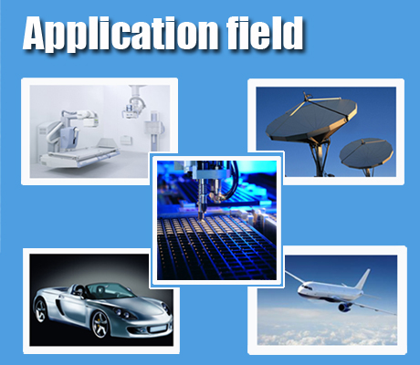
High-frequency multilayer PCBs are engineered for GHz-level signal transmission used in 5G communication, automotive radar, satellite systems, and aerospace electronics.
Unlike standard FR-4 PCBs, high-frequency boards require strict control of:
- Dielectric constant stability (Dk)
- Signal loss (Df)
- Impedance control (50Ω / 75Ω)
- Multilayer alignment accuracy
👉 In real manufacturing experience, over 80% of RF PCB failures are caused by material mismatch and lamination instability, not circuit design errors.
1. High-Frequency PCB Material Selection
High-frequency PCB performance depends primarily on substrate material.
Common RF Materials:
- Rogers RO4350B / RO4003C
- PTFE (Teflon-based laminates)
- Taconic RF series
- Shengyi high-frequency laminates
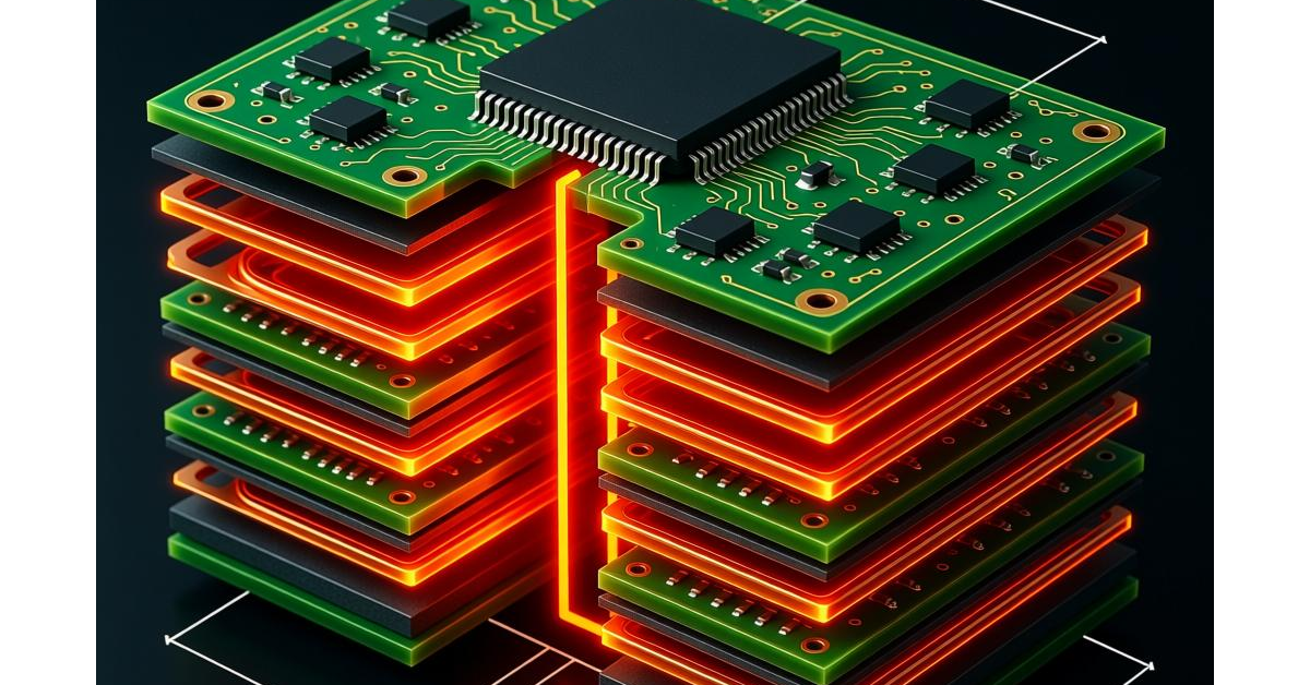
High-Frequency PCB Stack-Up Structure
ALT: high frequency PCB multilayer stack-up structure showing impedance controlled routing layers
Key Engineering Insight
Material mismatch (especially FR-4 + PTFE) is the leading cause of delamination in multilayer RF PCBs.
Best Practices:
- Use high-Tg prepreg (≥170°C)
- Avoid direct FR-4/PTFE bonding
- Perform DFM stack-up simulation
External Reference Links
PCB Manufacturing Process
High-Frequency PCB Capability
2. High-Frequency Lamination Process
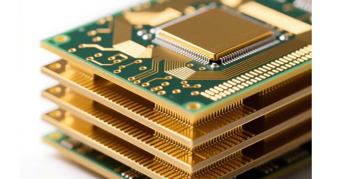
Vacuum Lamination Process
ALT: vacuum lamination process for multilayer high frequency PCB manufacturing
Process Steps:
- Vacuum de-airing
- Stepwise temperature ramp-up
- Multi-stage pressure control
Engineering Rule:
- Low temperature → incomplete curing → delamination
- Uneven pressure → trapped air → signal loss
Layer Alignment Control
- Shrinkage compensation modeling
- Pin-lamination system
- Thermal expansion correction
👉 Target accuracy: ±25 μm
3. Drilling & Via Reliability Engineering
High-frequency materials such as PTFE and Rogers are mechanically soft and thermally sensitive.

CNC Drilling Process
ALT: CNC drilling process for high frequency PCB via formation
Key Challenges:
- Resin smear
- Via roughness
- Drill bit wear
Engineering Solutions:
- Micro-grain carbide drills
- Plasma desmear process
- Optimized chip evacuation
4. Electroplating & Etching

VCP Plating Line
ALT: VCP vertical continuous electroplating line for high frequency PCB via metallization
Key Technologies:
- VCP (Vertical Continuous Plating)
- Pulse plating
- Controlled copper distribution
Control Target:
- Copper thickness variation <10%
- Impedance tolerance ±5%
Etching Process Optimization
- Laser Direct Imaging (LDI)
- Etching compensation control
- Fine line width control (±0.02mm)
5. Quality Control System

PCB Cross Section Inspection
ALT: PCB cross section analysis showing via copper thickness and multilayer bonding quality
Testing System Includes:
- TDR impedance testing (100% critical traces)
- Thermal stress test (288°C × 3 cycles)
- Cross-section metallography
6. Engineering Experience
Based on real production data:
High-frequency PCB performance is determined more by manufacturing consistency than circuit design complexity.
The 3 Core Factors:
- Material compatibility
- Lamination stability
- Impedance control precision
7. Internal Link Cluster
- PCB Manufacturing Process
- High Frequency PCB Overview
- Manufacturing Capability
- PCB Resources
- About Company
- Contact Engineering Team
8. Conclusion
High-frequency multilayer PCBs are precision-engineered systems designed for:
- Low-loss signal transmission
- Stable impedance control
- High-frequency electromagnetic compatibility
They are essential for:
- 5G communication systems
- Automotive radar
- Satellite communication
- Aerospace electronics