
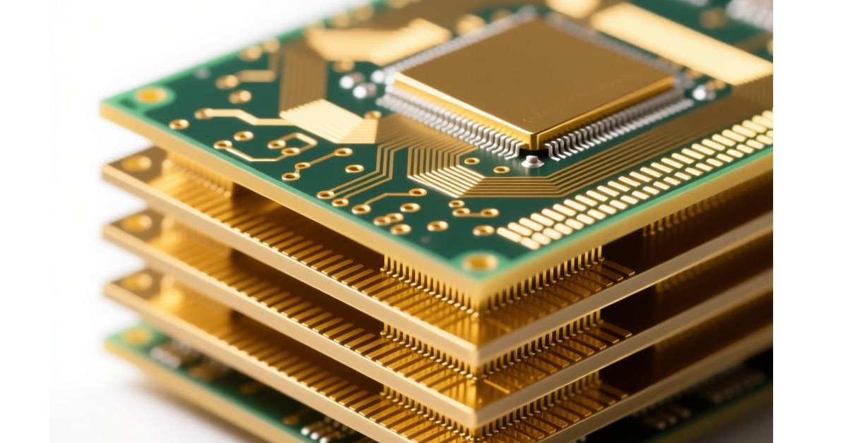
In the current era of global transformation driven by artificial intelligence, we are captivated by the capabilities of large language models, the advancing technology of self-driving cars, and the accuracy of smart recommendations. However, the physical heart that powers these digital intelligent systems is not just made of algorithms, but of sophisticated hardware—specifically, the high-frequency printed circuit boards that facilitate all computation and communication. The AI sector’s relentless pursuit of greater data processing speeds, higher transmission bandwidth, and increased component density has elevated the manufacturing requirements for high-frequency PCBs to a level that far surpasses conventional specifications.
To understand these rigorous demands, it is essential to recognize the core need of AI hardware: to process and move immense volumes of data as quickly as possible, using the least amount of energy. This fundamental requirement creates significant challenges for PCBs in three key areas: signal integrity, power integrity, and thermal management.
I. The Material Foundation: A Battlefield Defined by Low Loss and High Stability
Standard FR-4 substrate material, common in consumer electronics, becomes a liability when faced with the high-frequency, high-speed signals essential for AI. Within AI servers and switches, the data streams traveling between components like GPUs, CPUs, and network interfaces are now routinely operating at 112 Gbps, with the industry rapidly moving toward 224 Gbps. At these frequencies, signal loss as it travels through the PCB material becomes a critical obstacle.
Consequently, selecting materials with a low dielectric constant and an exceptionally low dissipation factor is paramount. Leading manufacturers turn to specialized high-frequency substrates from suppliers like Rogers, Panasonic (with its Megtron series), and Taconic. These advanced materials significantly reduce signal energy loss and propagation delay, ensuring data can be transmitted efficiently over longer distances on the board. It is equally critical that the dielectric constant of these materials remains stable despite changes in frequency or temperature. This stability is the foundation for maintaining consistent signal impedance and preventing waveform distortion; even minor inconsistencies can lead to a sharp increase in data errors.
Additionally, due to the “skin effect,” high-frequency electrical currents travel primarily along the outer surface of a conductor. This makes the smoothness of the copper foil a direct factor in signal loss. AI-grade PCBs require the use of very low-profile or reverse-treated copper foils, where the exceptionally smooth side is used for carrying signals. This minimizes energy loss and signal distortion caused by a rough conductive surface.
II. Precision Manufacturing: An Exercise in Micron-Level Accuracy
If advanced materials provide the foundation, then precision manufacturing is the process that turns that foundation into a high-performance component. Producing PCBs for AI hardware is a discipline that operates at a micron scale.
First, impedance control must be exceptionally strict. High-speed signals are highly sensitive to impedance mismatches. Any discontinuity acts like an echo, reflecting part of the signal back and corrupting the data stream. This necessitates extremely tight tolerances for trace width, trace spacing, and dielectric thickness, typically within ±5% or less. Achieving this demands masterful control over imaging, etching, and lamination processes.
Second, high-density interconnect and microvia technology are essential. Modern AI chips, packed with billions of transistors, connect to the rest of the system via thousands of pins. The PCB must provide a vast number of extremely small vertical connections to facilitate this. Laser drilling is used to create micro-vias with diameters as small as 50 micrometers. A subsequent challenge is ensuring these deep, narrow holes are uniformly plated with copper, a process that tests the limits of electroplating technology.
Finally, back-drilling is a non-negotiable process. In a multi-layer PCB, the unused portion of a through-hole via forms a copper stub. This stub acts as an antenna, resonating at specific frequencies and causing significant signal degradation. Back-drilling precisely removes this unused portion of the copper barrel, cleaning up the signal path. It is a standard and critical step in manufacturing PCBs for high-performance AI computing and networking equipment.
III. System-Level Co-Design: Bridging the Gap Between Functionality and High Performance
A perfectly manufactured PCB does not, by itself, guarantee a high-performing system. True success requires deep collaboration between design and manufacturing, validated by rigorous simulation and testing.
Effective thermal management is a critical lifeline. AI processors often consume hundreds of watts of power, generating immense heat that must be drawn away immediately. This has led to innovative PCB-integrated cooling solutions, such as embedded heat pipes or metal cores, the use of substrates with high thermal conductivity, and thick copper power planes. The PCB thus evolves from a simple interconnection platform into an active element of the thermal management system.
The choice of surface finish also impacts performance. The traditional Hot Air Solder Leveling finish is unsuitable due to its uneven surface. Modern AI hardware utilizes flatter finishes like Electroless Nickel Immersion Gold or immersion silver, which provide a more uniform surface for soldering and improved signal integrity at high frequencies.
Most importantly, a co-design philosophy integrating Design for Manufacturability and system-level simulation is mandatory from the outset. PCB designers must work closely with fabricators, considering manufacturing capabilities and material behaviors during the initial design phase. They must also employ advanced simulation tools to model and optimize signal and power integrity before the board is ever built, ensuring the final product performs as intended in the real world.
Conclusion
In summary, the demands placed on high-frequency PCBs by the AI industry can be described as a relentless drive toward higher performance, greater precision, and superior stability. This drive is propelling continuous innovation across material science, precision engineering, and electronic design automation. Companies that can master these demanding requirements occupy the top tier of the global electronics manufacturing ecosystem. In the ultimate race for computational supremacy, every high-frequency PCB embedded within an AI server acts as a silent, indispensable foundation stone for the modern intelligent revolution. They stand as a testament to a fundamental truth: in the age of AI, the physical limits of hardware ultimately determine the scope of what intelligence can achieve.