
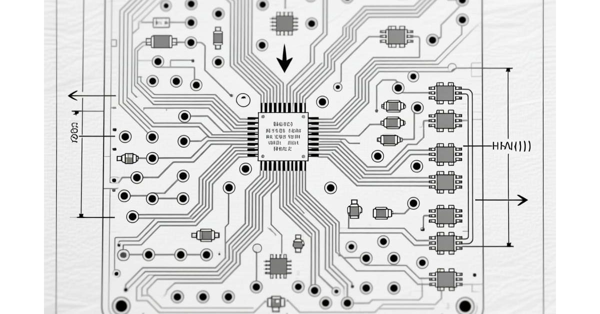
Driven by high-performance computing, artificial intelligence, and 5G communications, high-frequency circuit boards have evolved from ordinary circuit carriers into key functional components that define system performance. As traditional manufacturing methods approach their physical limits, achieving a new balance between signal integrity, reliability, and cost requires fundamental breakthroughs and innovations across the entire production chain, from raw materials to final packaging.
Breakthrough One: The Shift from Standard Substrates to Advanced Materials Engineering
While traditional manufacturing begins with ready-made copper-clad laminates, modern innovation starts much earlier, in the phase of material customization.
- Nanoscale Engineering of Dielectric Materials: The future lies in designing and controlling dielectric materials at the molecular level. Utilizing nanoceramic filler technology, inducing the oriented alignment of liquid crystal polymers, and developing next-generation ultra-low-loss thermoset resin systems allow for precise tuning of dielectric constant stability and minimizing dielectric loss. This goes beyond simply reducing loss; it aims for exceptional consistency in electrical properties across varying frequencies and temperatures, a critical requirement for broadband millimeter-wave applications.
- Achieving Atomically Smooth Copper Interfaces: Since millimeter-wave signals travel primarily along the conductor surface (the skin effect), the copper foil’s smoothness is paramount. Innovations focus on advanced Hyper Very Low Profile and reverse-treated copper foils. These are combined with plasma or chemical nanotexturing techniques that ensure strong adhesion to the resin while achieving sub-micron surface smoothness, dramatically reducing signal path loss.
- Integration of Multifunctional Materials: Innovation involves building functionality into the board’s structure. This includes laminating insulating layers pre-filled with high-thermal-conductivity particles or incorporating metal-core or ceramic-core materials with matched thermal expansion in strategic layers. This “integrated structural cooling” approach tackles the heat dissipation challenges of high-power chips at the source.
Breakthrough Two: From Geometric Shaping to Electromagnetic Performance Machining
Core processes like drilling and circuit patterning are undergoing a paradigm shift. The goal is no longer just to create physical shapes but to precisely engineer electromagnetic behavior.
- The Microvia Revolution via Advanced Lasers: Vias are critical impedance discontinuities in high-speed channels. The innovation is using ultraviolet and ultrafast picosecond lasers to create micro-blind and buried vias. By controlling drill taper, depth, and wall smoothness with extreme precision and pairing this with advanced via filling and conformal plating, signal reflection and loss are minimized to meet the demands of ultra-high-density interconnects.
- The Pursuit of Ultra-Precise and Consistent Circuit Formation: For differential lines carrying 112Gbps+ signals, tolerances for line width and spacing are now as tight as ±2%. This necessitates co-optimization of high-precision Direct Laser Imaging optics, specialized photoresist chemistries, and dynamically controlled fine-line etching processes. The emerging trend is deploying AI-powered real-time monitoring systems that adjust for process variations, ensuring absolute impedance uniformity across the entire board.
- Adopting Signal-Friendly Surface Finishes: Traditional surface finishes like Electroless Nickel Immersion Gold can degrade signal quality at ultra-high frequencies due to increased skin effect loss. The innovation path leads toward ultra-flat, low-cost immersion silver finishes and the development of specialized Organic Solderability Preservative formulations. These alternatives provide a smoother, lower-loss surface for high-frequency signals while maintaining excellent solderability.
Breakthrough Three: From Isolated Processes to System-Level Co-Design Fusion
The most transformative innovations are emerging at the intersections where PCB manufacturing converges with chip design and packaging.
- Heterogeneous Integration with Advanced Packaging: With the rise of Chiplet and silicon photonics technologies, the PCB’s role is expanding. It is becoming a package-level interconnect substrate. Innovations here involve substrate-like manufacturing processes capable of producing line widths of 15μm or less and extremely fine microvias. Techniques like the Semi-Additive Process and embedded component technology allow passive components and even active chiplets to be buried within the board, shortening critical electrical paths and boosting overall system performance.
- The Intelligent DFM Closed Loop: Leveraging Generative AI and digital twin simulations, manufacturers can now perform comprehensive electromagnetic, thermal, and stress analyses before any physical production begins. Crucially, real-world manufacturing data on etch rates, lamination thickness, and other parameters can be fed back into the design loop. This creates an intelligent design-simulation-manufacturing-feedback cycle that drastically improves first-pass success rates, a major innovation for cost control.
- Data-Driven, Full-Process Quality Transparency: Moving beyond random destructive testing, innovation introduces inline terahertz time-domain spectroscopes and microwave probe systems. These tools perform non-destructive, full-field inspections at key stages, measuring dielectric properties, impedance, and loss across the entire board. This builds a comprehensive “quality data map” for each board, enabling a shift from inspecting final results to predicting and controlling quality throughout the process.
In summary, innovation in high-frequency PCB manufacturing is no longer about incremental improvements to individual steps. It represents a systemic revolution that spans materials science, precision engineering, electromagnetics, and data intelligence. The core philosophy is evolving from passively shaping generic materials to actively constructing sophisticated, performance-optimized structures. Success in this new era depends on mastering material interfaces at the nanoscale, controlling signal paths at the micron scale, and fostering seamless collaboration across the entire system design chain. This endeavor is not merely a technical hurdle; it is a pivotal strategic opportunity to redefine the value proposition and future of electronic hardware.