
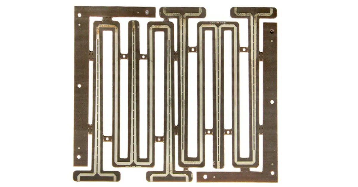
Double-sided multilayer PCBs are widely used in modern electronic devices, especially in scenarios with complex circuits and high-density interconnections. Compared with single-layer PCBs, double-sided multilayer PCBs have a more complex manufacturing process, involving lamination, drilling, etching, copper deposition, and pad plating, among others. Below is a detailed introduction to the production process and key considerations for double-sided multilayer PCBs.
I. Key Production Processes
Material Preparation The production of double-sided multilayer PCBs begins with selecting suitable substrate materials. Commonly used materials include FR4, aluminum substrates, and copper substrates, with choices based on electrical, thermal, and mechanical properties. Different layer counts and thicknesses may require varying specifications of copper foil, prepreg (PP), and inner layer materials to ensure the final product’s durability and conductivity.
Inner Layer Fabrication In multilayer boards, inner layer fabrication determines the board’s electrical performance. Key steps include cleaning, pattern transfer, etching, cleaning, and AOI inspection. Due to the complexity of double-sided multilayer board circuits, precise control over etching speed and depth is necessary to avoid short circuits or open circuits. Automated Optical Inspection (AOI) equipment is used to detect small defects and ensure inner layer integrity.
Lamination Process The lamination process combines each inner layer, copper foil, and insulating materials into a single unit by heating and pressing. Temperature, pressure, and timing are critical, ensuring bonding strength and alignment accuracy between layers. Multilayer PCB lamination typically involves sequential lamination under specific pressure and temperature to avoid air bubbles or delamination.
Drilling Drilling is key to creating interlayer connections. Drilling in double-sided multilayer PCBs requires high precision because any misalignment or burr can cause signal transmission issues. CNC drilling machines are typically used, and in some cases, laser drilling is employed for higher hole wall smoothness and accuracy. For micro-holes, blind vias, and buried vias, laser drilling is especially essential.
Chemical Copper Deposition and Electroplating In double-sided multilayer PCB production, chemical copper deposition forms a thin copper layer on non-conductive surfaces, creating pathways between layers. After chemical copper, copper electroplating thickens the copper layer to enhance conductivity. This process requires precise control over the concentration and temperature of chemical solutions to avoid uneven copper layers, which can affect solderability and signal transmission.
Outer Layer Pattern Transfer and Etching Pattern transfer for outer layers typically uses photolithography and dry film technology to transfer patterns to the PCB surface, followed by etching to remove unwanted copper. Accurate etching is essential to meet design specifications for line width and spacing, avoiding short circuits and electrical failures.
Surface Treatment Surface treatment for double-sided multilayer PCBs mainly enhances oxidation resistance and solderability. Common processes include Hot Air Solder Leveling (HASL), chemical silver plating, and chemical gold plating. Chemical gold plating is widely used in high-performance PCBs for its excellent oxidation resistance and conductivity.
Inspection and Quality Control Inspection and quality control are essential in double-sided multilayer PCB production, involving electrical testing, visual inspection, AOI, and interlayer alignment checks. Electrical testing ensures that circuit continuity and impedance meet requirements, while X-ray inspection can verify alignment accuracy in blind/buried vias and interlayer alignment for board reliability.
II. Precautions During Processing
Temperature Control Temperature control is crucial in lamination, drilling, and plating steps. Excessive temperatures may cause substrate delamination or deformation, while low temperatures may lead to poor adhesion. Strict temperature control, especially in lamination, ensures bonding strength between layers.
Humidity Control Substrates are sensitive to humidity, which can increase the dielectric constant of insulating materials and impact signal quality. Low humidity in the production environment helps prevent moisture absorption, ensuring dimensional stability and maintaining dielectric properties.
Impedance Control Impedance control is crucial in double-sided multilayer PCB design. Selecting suitable materials, layer spacing, line width, and etching processes effectively controls signal impedance to ensure consistent circuit performance. Impedance testing further confirms whether impedance requirements are met.
Hole Quality Management Hole quality is vital in multilayer PCBs, especially for blind and buried vias. Rough hole walls or uneven diameters can impact solder quality and electrical connectivity. By selecting appropriate drilling processes, optimizing drilling parameters, and electroplating holes, the conductivity and reliability of holes can be improved.
Interlayer Alignment Precision Interlayer alignment precision in double-sided multilayer PCBs directly affects stability, particularly in the distribution of signal and ground layers. Misalignment can cause signal interference and transmission instability. Optical alignment and automatic adjustment during lamination and stacking help maintain alignment accuracy.
Electrostatic Protection Static electricity can damage electronic components or reduce PCB performance. Anti-static measures, such as anti-static wristbands and mats, should be used during production to reduce the impact of static electricity on the PCB.
Chemical Selection and Handling Double-sided multilayer PCB manufacturing involves numerous chemical processes, such as etching and plating. The purity and stability of chemical reagents are essential to ensure quality in each step. Attention to chemical handling and waste disposal is also necessary to meet environmental standards.
Environmental Protection and Safety The double-sided multilayer PCB manufacturing process involves some harmful chemicals and exhaust gases, so effective emission measures are essential. Installing ventilation and waste liquid treatment systems ensures production safety and environmental protection.