
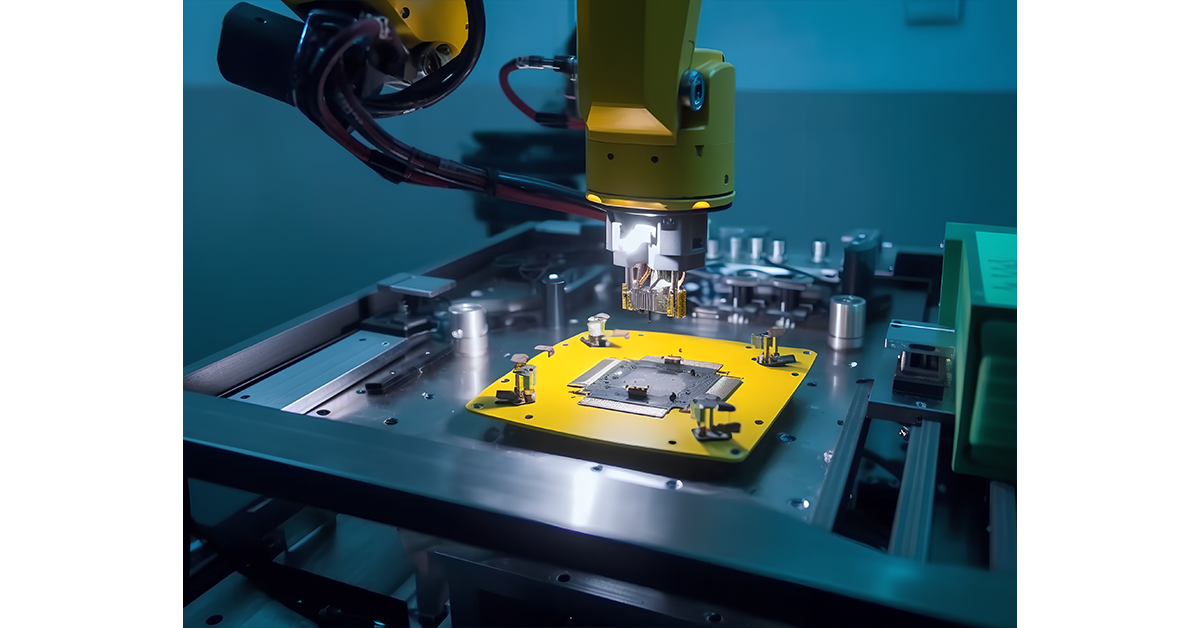
To manufacture a circuit board that meets the stringent demands of high-frequency applications—such as 5G, millimeter-wave radar, or AI servers—involves a series of highly precise processes. Each step, from transferring the design pattern onto the substrate to drilling micro-vias finer than a human hair and laminating multiple layers, requires specific, professional equipment. This specialized toolchain is essential to guarantee the final product’s low signal loss and high reliability.
For a clear overview, here is a summary of the key equipment aligned with the core production stages:
1. Pattern Formation and Transfer
This initial stage creates the circuit pattern on the board.
- Laser Direct Imaging (LDI) Machine: Uses a laser to directly “draw” precise circuit patterns onto a panel coated with photoresist, offering superior accuracy essential for fine lines.
- UV Exposure Unit: A traditional yet critical tool that transfers the pattern from a film to the photosensitive board using ultraviolet light.
- Etching and Developing Line: Employs chemical solutions to selectively remove copper, forming the final conductive traces after the pattern is defined.
2. Precision Drilling
This stage creates the holes for vertical electrical connections between layers.
- High-Speed CNC Drilling Machine / Laser Drilling Machine: Uses high-speed drill bits or focused laser beams to create micro-vias. Mechanical drill spindle speeds can reach several hundred thousand RPM, while lasers produce the finest micro-vias.
3. Multi-layer Lamination
This process bonds multiple circuit layers into a single, solid board.
- Vacuum Laminating Press: Applies precise heat and uniform pressure under a vacuum to bond layers of core material and prepreg into a monolithic structure without air entrapment.
4. Hole Metallization and Plating
This critical step makes the drilled holes electrically conductive.
- Electroless Copper Deposition Line (PTH Line): Chemically deposits a thin, foundational layer of copper onto the non-conductive hole walls, enabling subsequent electroplating.
- Electroplating Line: Electrochemically builds up and thickens the copper layer on the hole walls and surface traces to ensure proper conductivity and reliability.
5. Surface Finish and Solder Mask Application
This stage prepares the board for component assembly and protects the circuitry.
- Surface Finish Line: Applies a final coating—such as Electroless Nickel Immersion Gold (ENIG) or Immersion Silver—to exposed copper pads to ensure solderability and prevent oxidation.
- Solder Mask Printing and Exposure Equipment: Applies, patterns, and cures the insulating solder mask ink to protect copper traces.
6. Routing, Testing, and Quality Control
The final steps shape the board and verify its quality and performance.
- CNC Routing Machine: Cuts individual boards from the larger production panel to their final outline.
- Flying Probe / Bed-of-Nails Tester: Electrically tests all circuits for opens, shorts, and connectivity.
- Automated Optical Inspection (AOI) System: Uses cameras to automatically scan for surface defects.
- Impedance Tester: Measures the impedance of critical signal traces to ensure they meet high-speed design specifications.
Key Differentiators for High-Frequency Production
Manufacturing high-frequency boards imposes stricter demands than standard PCB production:
- Extreme Precision: High-frequency signals are sensitive to impedance, requiring tight control over trace geometry. This demands micrometer-level accuracy from LDI and etching systems, and high-precision drilling capable of sub-0.1mm holes.
- Specialized Material Handling: Materials like PTFE are soft and heat-sensitive. A vacuum laminating press with excellent temperature uniformity and pressure control is vital to prevent delamination or warping.
- Advanced Cleaning and Testing: Minute contaminants can disrupt signals, making plasma cleaners important. For performance validation, a High-Frequency Vector Network Analyzer (VNA) is key for directly measuring signal loss and phase characteristics.
Considerations for Equipment Planning
Selecting equipment requires a balanced approach:
- For R&D/Prototyping: Focus on flexible setups like an LDI machine, rapid etching line, and flying probe tester.
- For High-Volume Production: Investment in full, automated lines with high-precision, stable equipment from leading brands for core processes is necessary.
- Cost-Benefit Balance: Ensure performance in critical steps, but consider cost-effective options for supportive, non-core processes.
In summary, high-frequency circuit board production is a precision system. Its equipment chain is designed to meet the challenges of high precision, consistency, and specialized material handling to ensure stable, efficient signal transmission. A deep understanding of this equipment is fundamental for effective production planning and quality assurance.