
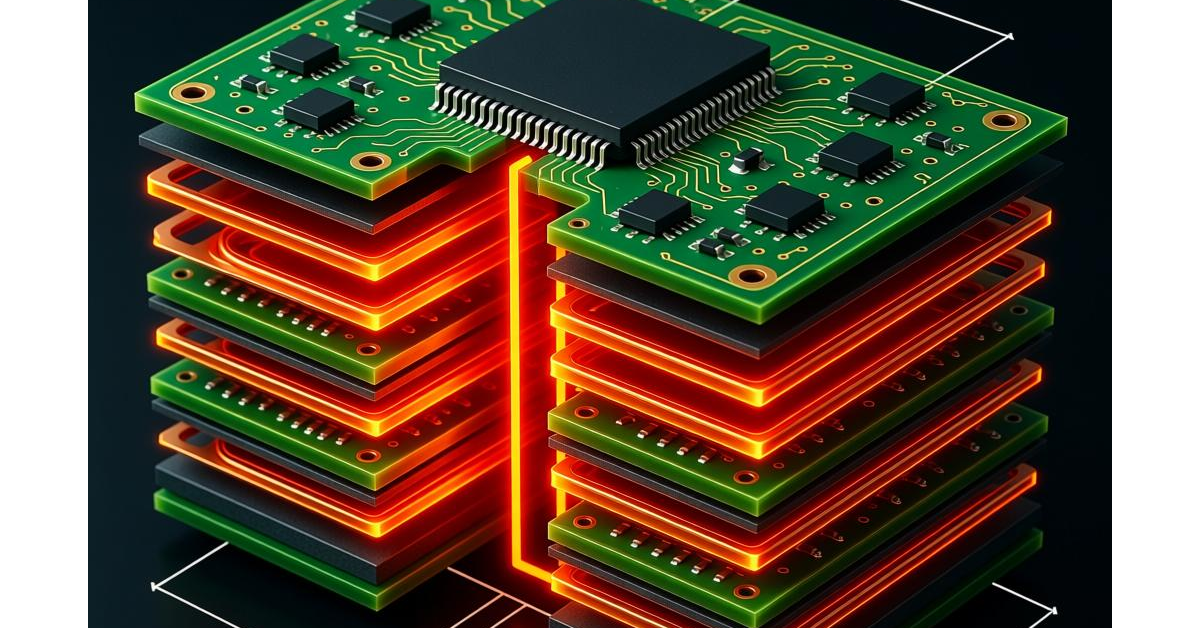
In high-frequency PCB (printed circuit board) manufacturing, engineers often face a critical choice between laminating multiple layers into a single board versus processing layers separately and assembling them later. This decision significantly impacts performance, reliability, cost, and manufacturability. Below is a detailed comparison of the challenges and key considerations for each approach.
Option 1: Laminated Multilayer Boards (All Layers Bonded Together)
This traditional method involves stacking and bonding three or more circuit layers into a unified board using heat and pressure.
Key Challenges:
- Material Consistency: All substrate and prepreg layers must have nearly identical dielectric properties. Even minor variations in dielectric constant (Dk) or dissipation factor (Df) can cause impedance mismatches and signal integrity issues.
- Precision Alignment: Layer-to-layer registration must be extremely accurate (often within ±0.05mm) to avoid impedance discontinuities and signal reflection, especially for high-speed or RF designs.
- Drilling and Plating: Creating reliable microvias and through-holes in a thick, multilayered stack is difficult. Issues like “drill smear,” incomplete plating, or uneven copper deposition can degrade electrical performance.
- Thermal and Mechanical Stress: Different materials may have mismatched coefficients of thermal expansion (CTE). During lamination, this can lead to warping, delamination, or residual stress, affecting long-term reliability.
Processing Considerations:
- Use high-frequency laminates from the same batch to ensure consistent electrical properties.
- Implement strict process controls for lamination pressure, temperature, and vacuum to prevent voids or resin-rich areas.
- Employ advanced laser drilling and plasma desmear for clean, reliable vias.
- Include impedance test coupons and perform thorough electrical testing to validate signal integrity.
Option 2: Separately Processed and Assembled Layers
In this approach, each layer or sub-board is fabricated individually and later assembled using connectors, bonding films, or mechanical fasteners.
Key Challenges:
- Interlayer Connection and Alignment: Precisely aligning and electrically connecting separate boards is complex. Misalignment can cause impedance jumps, crosstalk, or signal loss.
- Interface Management: Air gaps, adhesive layers, or connectors between boards create discontinuities in the signal path. These must be carefully modeled and controlled to minimize reflections.
- Mechanical Stability: Assembled boards may be less rigid and more prone to vibration, shock, or thermal cycling failures unless adequately secured.
- Thermal Management: Heat dissipation can be less efficient across assembled interfaces, requiring careful thermal design.
Processing Considerations:
- Design precision alignment features (e.g., dowel pins, guide holes) into each sub-board.
- Select bonding materials or connectors with matched impedance and stable high-frequency performance.
- Use electromagnetic simulation to model and optimize interlayer transitions.
- Consider mechanical reinforcements or enclosures to enhance robustness in demanding environments.
How to Choose Between the Two Methods?
- Choose laminated multilayer boards when:
You need the best possible signal integrity, high reliability, and compact form factor. This method is ideal for high-volume production of optimized designs, such as in 5G infrastructure, aerospace, or advanced radar systems. - Choose separately assembled layers when:
You require design flexibility, easier prototyping, or the ability to replace or upgrade individual sections. This approach is suitable for R&D, low-to-medium volume production, or hybrid designs combining different materials or technologies.
Final Recommendation:
The choice ultimately depends on your performance targets, budget, timeline, and production scale. Laminated boards offer superior electrical performance but require advanced manufacturing capabilities. Separately processed layers provide greater flexibility and easier debugging but introduce additional interface challenges. Careful design for manufacturability (DFM) and close collaboration with your PCB supplier are essential for success in either case.