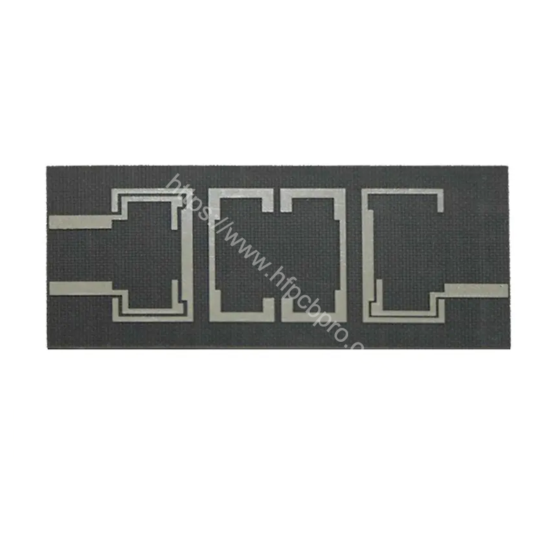
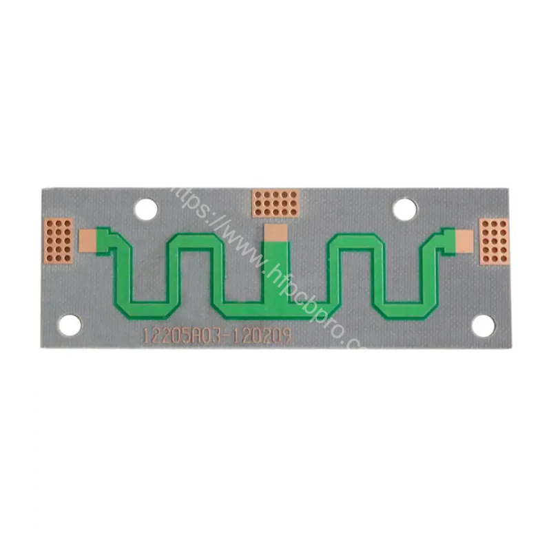
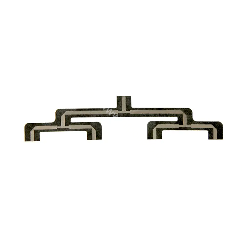
F4BTMS350 Aerospace Navigation PTFE PCB is a high-performance solution designed for High Frequency PCB > F4B PCB applications. Key features include Number of layers: 16, Dissipation Factor (Df): 0.0016.
| Number of layers | 2L |
|---|---|
| Material | WangLin F4BTMS350 |
| Board Thickness | 0.127mm(5mil) |
| Copper Thickness | 1/1oz(35um) |
| Surface Treatment | IPC6012 Class 3 |
| Dielectric Constant (Dk) | 3.50 @10GHz |
| Dissipation Factor (Df) | 0.0016 @10GHz, 0.0019 @20GHz, 0.0024 @40GHz |
| Product Type | Aerospace Navigation |
F4BTMS350 Aerospace Navigation PTFE PCB is a premium choice in the field of High Frequency PCB > F4B PCB, High Frequency PCB, Multilayer PCB, RF Micorwave PCB, High Frequency PCB > Rogers PCB. It offers exceptional performance with Number of layers: 2, ensuring reliability and efficiency for critical applications. Designed for Aerospace Navigation, this product excels in Dissipation Factor (Df): 0.0016. With advanced technology, it meets the demands of High Frequency PCB > F4B PCB, High Frequency PCB, Multilayer PCB, RF Micorwave PCB, High Frequency PCB > Rogers PCB, providing unparalleled quality. Perfect for professionals requiring high-frequency or specialized circuit performance, it remains an industry-leading solution in Product Type.
F4BTMS350 Aerospace Navigation PTFE PCB is designed for high-frequency aerospace navigation, RF microwave communication and precision signal transmission applications. Built with WangLin F4BTMS350 PTFE-based laminate, this 2-layer PCB provides stable dielectric performance with Dk 3.50 at 10GHz and low dissipation factor values of 0.0016 at 10GHz, 0.0019 at 20GHz and 0.0024 at 40GHz.
With a thin 0.127mm / 5mil board thickness and 1oz copper on both sides, this F4B PTFE PCB is suitable for compact RF layouts, aerospace navigation modules, satellite navigation systems, avionics communication circuits and other high-frequency applications where low signal loss and stable impedance are required.
The material’s low-loss PTFE characteristics help maintain signal integrity at microwave frequencies, while the 2-layer structure supports efficient RF routing and controlled impedance design. It is suitable for engineers developing lightweight, high-reliability RF circuit boards for aerospace, navigation, communication and defense-related electronic systems.
We offer a variety of high-frequency materials, including Rogers (e.g., RO4350B, RO5880), Taconic, and PTFE, depending on customer requirements.
Absolutely, we can provide detailed datasheets for review.
Our high-frequency PCBs can support frequencies up to 110 GHz, depending on the design and materials used.
We ensure precise impedance control through accurate stackup design, detailed impedance simulations, and advanced manufacturing processes.
Yes, we can combine materials like FR4 and high-frequency laminates for hybrid PCBs.
Restrictions mainly involve minimum trace width/spacing and material selection, depending on your design requirements.
We enhance thermal performance by using high thermal conductivity materials (e.g., metal-based PCBs) and optimizing copper thickness.
Thermal conductivity ranges from 0.2 W/m·K to 1.0 W/m·K, depending on the material.
ENIG/Gold Plating/Immersion Silver/Silver Plating/HASL/Gold finger/OSP/Nickel-palladium Gold/Resin plugging/Countersinking/ENIG+Hard Gold Plating/ImNi+ImTin/ENIG+OSP
ENIG is recommended due to its flat surface and excellent conductivity for high-frequency use.
We can produce high-frequency PCBs with layers ranging from 2 to 72.
Yes, we specialize in multilayer high-frequency PCBs and support hybrid stackup processes.
The thickness tolerance is ±0.05 mm, and the trace width tolerance is ±10%.
We perform impedance testing, RF performance testing, vacuum thermal testing, and more.
We achieve this by using high-quality materials, optimized manufacturing processes, and strict control of board thickness and other parameters.
Answer: Prototypes typically take 2–7 business days, while mass production takes 6–15 business days, depending on order volume and complexity.
High-frequency materials (e.g., Rogers) are more expensive, and higher layer counts increase complexity and cost.
We ensure reliability by using high-quality materials, rigorous testing, and optimized manufacturing processes.
Yes, our PCBs can endure temperatures up to 260°C and are suitable for harsh environments.
We use anti-static bags, vacuum packaging, and shockproof padding in the outer cartons for protection.
We provide air freight, express delivery, and sea shipping, depending on your needs, DHL is always prefered that ensure timely delivery through reliable logistics.